2.0mm 4 Layer High Frequency PCB
High Frequency PCB 4 Layer High Frequency Printed PCB Rogers PCB White Solder Mask HF PCB Board
4 Layer High Frequency Printed PCB
High-frequency PCBs usually provide a frequency range from 500MHz to 2 GHz, which can meet the needs of high-speed PCB designs, microwave, radio frequency, and mobile applications. When the frequency is above 1 GHz, we can define it as high frequency.
The complexity of electronic components and switches is continually increasing nowadays and need faster signal flow rates. So, higher transmission frequencies are required. High-frequency PCBs help a lot when integrating special signal requirements into electronic components and products with advantages like high efficiency, and fast speed, lower attenuation, and constant dielectric properties.
High Frequency (HF) PCB is used to transmit electromagnetic waves in the frequency of GHz with minimal loses in the variety of applications, including mobile, microwave, radio frequency (RF) and high-speed design applications. Hence, printed circuit boards with some specific characteristics are used to transmit these electromagnetic waves. Several parameters are taken into considerations while designing a PCB for high frequency applications.
A high frequency PCB can meet your needs when incorporating a special signal requirement into your electronic devices and products. These higher transmission frequencies are capable of supporting the faster signal flow rates that are a necessity in today’s increasingly complex electronic switches and other components.
| Feature | Capability |
| Quality Grade | Standard IPC 2 |
| Number of Layers | 2- 24layers |
| Material | ROGERS, TACONIC, ARLON, FR4, |
| Board Size | Min 5mm x 5mm | Max 500mm x 745mm |
| Board Thickness | 0.2mm - 4.0mm |
| Copper Weight(Finished) | 0.5oz - 2oz |
| Min Tracing/Spacing | 3mil/3mil |
| Solder Mask Color | Green, White, Blue, Black, Red, Yellow... |
| Silkscreen Color | White, Black, Yellow... |
| Surface Finish | Electroless nickel/immersion gold (ENIG) - RoHS |
| Immersion silver - RoHS |
| Immersion tin - RoHS |
| Min Annular Ring | 0.1mm |
| Min Drilling Hole Diameter | 0.15mm |
| Other Techniques | Peelable solder mask |
| Gold fingers |
| Carbon oil |
| Countersink holes |
FAQ:
Q1:Are you a factory or trade company?
A: Yes, we are the factory, we have independent quick turn prototype PCB manufacturing & big volume PCB production lines.
Q2:What kind of PCB file format can you accept for production?
A: Gerber, PROTEL 99SE, PROTEL DXP, POWER PCB, CAM350, ODB+(.TGZ)
Q3:Are my PCB files safe when I submit them to you for manufacturing?
A: We respect customer's copyright and will never manufacture PCB for someone else with your files unless we receive written permission from your side, nor we'll share these files with any other 3rd parties. And we could sign NDA with client if necessary.
Q4:If we have no PCB file/Gerber file, only have the PCB sample,can you produce it for me?
A: Yes,we could help you to clone the PCB. Just send the sample PCB to us, we could clone the PCB design and work out it.
Q5:What is your standard lead time for PCB?
A: Sample/prototype(less than 3sqm):
1-2 Layers: 3 to 5working days (fastest 24hours for quick turn services)
4-8 Layers: 7~12 working days (fastest 48hours for quick turn services)
Mass production (less than 200sqm):
1-2 Layers:7 to 12 working days
4-8 Layers:10 to 15 working days
Q6:What payment do you accept ?
A: Wire Transfer(T/T) or Letter of Credit(L/C) or Paypal(only for small value less than 500usd)
Product Tags:

|
|
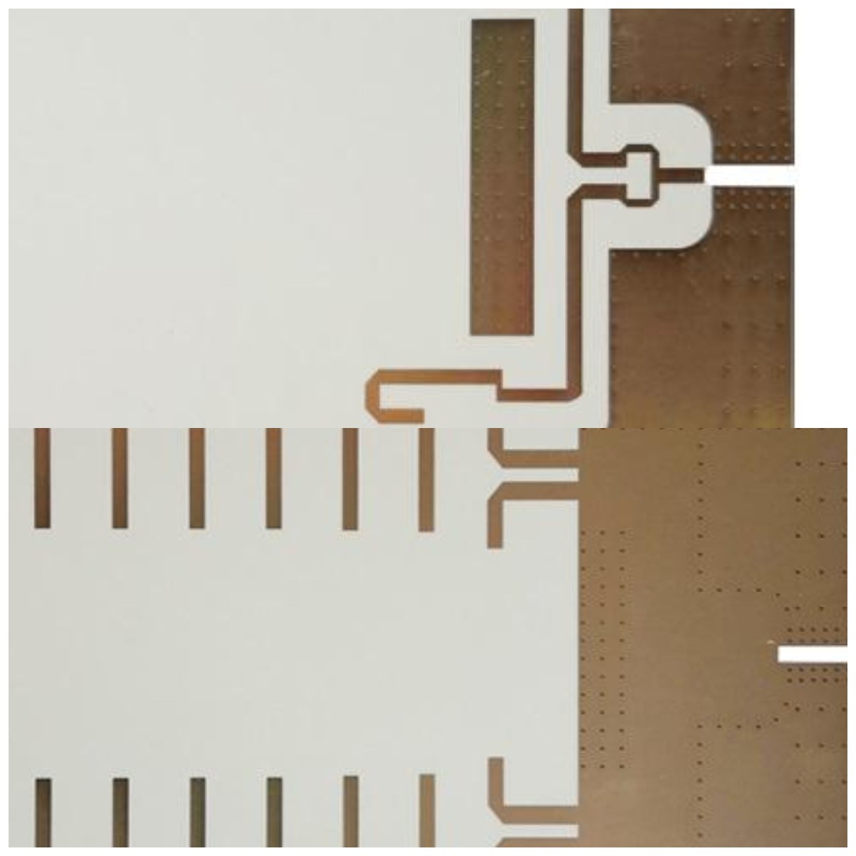
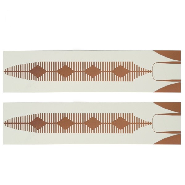
2.0mm 4 Layer High Frequency PCB Images
|